Electronics Forum

Electronics Circuits & Projects discussion forum. Get help with electronics.


Phototransistor switched Mosfet circuit design assistance

Discuss about electronic circuits here. Request help for circuits that you couldn't find anywhere else, how a circuit works etc. Discuss anything related to electronic circuits.

Moderator: pebe

Phototransistor switched Mosfet circuit design assistance

Postby capcouillon » Sat Nov 02, 2013 11:41 pm

As a non-EE or even hobbyist, I could use a hand working out the design of a simple "day/night" switch taking into account some fairly restrictive requirements. This is for a project that may require several hundred of the final design to be fabricated in house (In garage?) While I can read a schematic, and make a decent solder joint, my hardware expertise lies in the realm of bending moments and thread pitch, rather than ohms law and logic circuits.

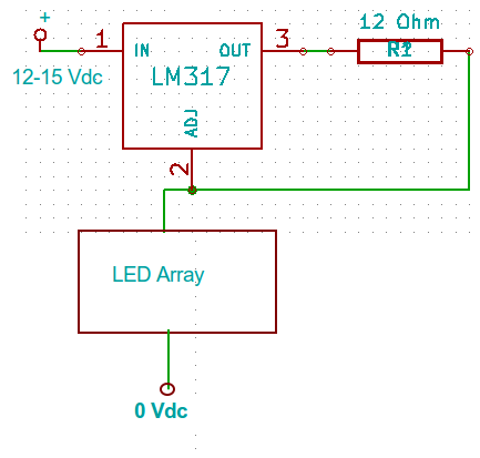
What we have is a fairly straight forward LED array that is being driven by a LM317 for current regulation. Source voltage ranges between 12-15 Vdc. The array housing which also will contain the electronics components is physically quite small (not by silicon standards, but everything is relative) with a volume of about 2.5 cubic inches. Power usage should be at an absolute minimum while being able to supply the required light output and pattern. As the entire housing will be filled with potting, heat generated by non-optimal component selection could present issues.

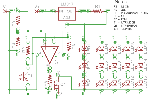
The basic array setup has proven simple, and several acceptable working prototypes have been build as below. The LM317 is set up for current regulation at 108 mA, and excess heat has not been an issue at this point. While voltage source will vary considerably over time, it is true DC, not cleaned up AC.

Image

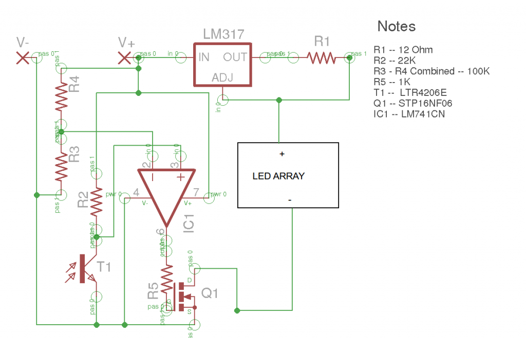
The next step in the project requires the integration of switch to control the above circuit, ie: Off at dawn, on at dusk. I have researched the options extensively but have run up against a number of issues which I am unable to resolve.
1. LDR or Phototransistor as detector?
2. Component cost and complexity exceeds build requirements.
3. Large variations in circuit parameters, none of which meet my build requirements and little additional info on modifying components to suit different voltages, loads, etc.
4. Use of electro-mechanical relays.
5. Lack of personal knowledge, and a good "Okie Inventory" of spare/used parts for experimentation. Need to whip up a jig out of some 3/8 304SS bar stock... got ya covered. Dig up some mosfets and a dozen various resistors? Not so much..

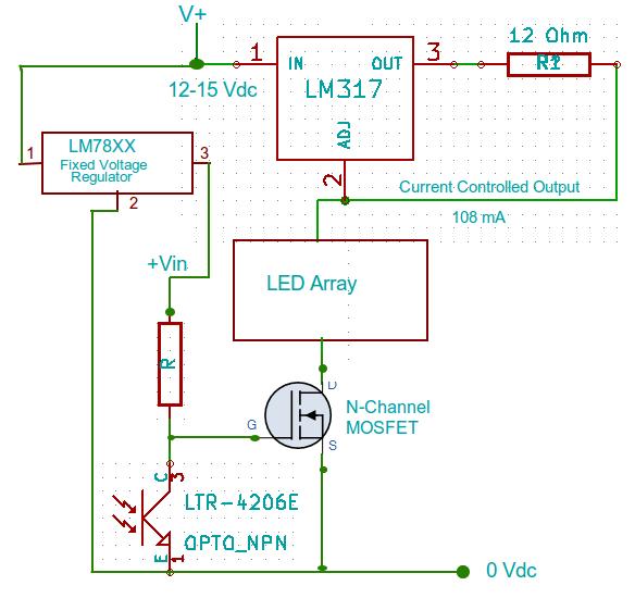
In particular light of issue #5 I have to do my engineering on paper before commiting to ordering parts. 100 mile round trip to the closest location I might find what I need, so Mouser is my friend. After some consideration I have arrived at a "plan" something like below. Justification of design parameters follows: Cad sulfide LDRs are getting harder to come by, and an IR range phototransistor has added advantage of not being as sensitive to non-solar, non-incandescent stray light at night. Mosfet "switch" should be inexpensive, and with I(d) at 108mA and a mosfet with an "on-resistance" in the range of 0.1 ohms, the power disipation should be less than 2 mW.
Not a lot of heat to get rid of. Added the LM78XX as I thunk it would be easier to create a stable voltage dependant control circuit if we had a standard voltage to start out with. Not large or expensive, but not sure of power disipation issues. Have concerns about what power the phototransistor will be passing during during daylight hours. Obviously less is better.

As I stated previously, my EE skills are somewhere between slim and none, and Slim's out of town... I figure the circuit below has an excellent chance of producing more laughs than required results as it has been cobbled up from what little I have been able to absorb during several weeks of searching for answers. The requirements for the circuit are pretty concrete, and I could use some specific concrete suggestions as to how to make it work as required. Eg: There is no part # for the mosfet. Mouser lists 3000+ thru-hole n-channel mosfets. Have a good suggestion for a part # that meets the requirements without having to sift the data-sheets? What voltage LM78xx should I use? Assume the closer I can get to the input voltage (less 1.25v) the less power dissipation I will have? Given the choice of voltage, what is a good starting value for the fixed resistance in the control circuit... and so on.

Image

Apologies for the long winded post, but figure I am not gonna get any specific answers without information as to the requirements.
Looking forward to suggestions and/or solutions that will yield better results.
capcouillon
 
Posts: 6
Joined: Sat Nov 02, 2013 11:32 pm

Re: Phototransistor switched Mosfet circuit design assistanc

Postby pebe » Sun Nov 03, 2013 12:27 pm

You have given a very comprehensive description of your needs, but a few more points need clarification.

You say everything will be contained within the LED array housing. Does that include the light sensor? If so, I assume it is clear – so is the potting compound translucent? Can you give more details?

Whatever potting compound you use, it will affect the heat dissipation from the components within. Could the design use a sealed box – rather than pot the components?

You haven’t given details of the LED array. Can you say what the voltage drop across it is, and at what current?

You mention LDRs are becoming difficult to find. But there are plenty on ebay like these, and dirt cheap!, so quantity deliveries should present no problem.

http://www.ebay.co.uk/itm/20pcs-Photore ... 4178b53292

On the question of power, can you be more specific about the source and the variable voltage limits it has? Is it a lead acid battery? You want to keep power to a minimum, so what is the maximum current that would be acceptable when the LEDs are off?

Knowing the answers to these will give a clearer picture of your needs.
pebe
 
Posts: 1058
Joined: Tue Dec 09, 2003 11:12 pm
Location: Ellon, Scotland

Re: Phototransistor switched Mosfet circuit design assistanc

Postby capcouillon » Sun Nov 03, 2013 3:08 pm

Housing is 1.5" PVC sched 40 pipe cap. 5mm leds are inserted from the inside via 5mm holes distributed around the circumference. 3mm phototransistor will be mounted in similar fashion in top portion of cap. Filled potting compound is used for enviromental exclusion and mechanical support. Inexpensive, reapeatable, low tech solution vs mechanical type mounting and seal. So far, power disipation has not been an issue as components are well matched, and working currents are low. If heat were to become an issue, thermo-conductive potting could be used, but at a cost increase. Better to improve circuit design than spend money on more potting, Heat is wasted energy.

Would prefer not to go into too many details about the array itself at this time. It should be sufficient to note total current 108 mA at a nominal 9.7 Vdc . Setup is stable and has currently been under test for 500+ hrs continious duty. At this level, the array is being driven at about 60% of rated max forward current.

Supply source is Lead/Acid flooded cell typical. Normal range 12.7 - 12.2 Vdc (100%-50% SOC). In severe discharge conditions (<25% SOC) Led combined Vf will exceed available supply and device will not function. Average terminal voltage during charge cycles 13.8Vdc although during equalization phases, voltages could range as high as 14.6 - 14.8 Vdc. Time spent in charging cycles dependent on too many outside factors to analyse here. For design calculations, we assumed 12.7 -12.2 Vdc 80% of the time.

During daylight hours with phototrasistor conducting and mosfet open, an idle current of less than 5ma would be good. 10ma would be acceptable.

Re: LDRs ... Agreed, there are lots of inexpensive Chinese LDRs available, but enviromental restrictions on the use of cadmium are reducing the available mfgs outside of Asia. As far as price, the LTR4206 spec't runs 9 - 14 cents (US) ea.

Have been continuing my research, and am looking at a STP16NF06 for the mosfet... Its overkill at 60V 16A but if I am reading the spec sheets right, DS resistance (on) is less than 0.1ohm and has a fairly wide range of V(gs) to play with. So it would seem to be down to determining the optimal voltage output for the LM78 (5,6,8,9,10 V) and matching it with the proper resistor ahead of the LTR.
capcouillon
 
Posts: 6
Joined: Sat Nov 02, 2013 11:32 pm

Re: Phototransistor switched Mosfet circuit design assistanc

Postby pebe » Sun Nov 03, 2013 5:33 pm

Hi. Your second post belies the modesty you claimed in your first post! It looks as though your ideas are pretty firmly fixed.

On the question of the FET though, your circuit will switch it too slowly. It needs to be switched on cleanly and that means going from Vgs = 0 to Vgs = 5V or more, to give it two defined states - on or off. So you will need to amplify the change of voltage across the phototransistor and use that to switch the gate.

The best way would be to use an op-amp (almost any type) with its supply fed from the full battery voltage. I would suggest putting a 22K resistor in series with the pt's collector and feeding that direct from your battery. Then take a feed from the collector to the non-inverting input of the op-amp. For the other input, wire a 100k pot across the battery supply and feed its wiper to the inverting input. When it gets dark the pt's collector voltage will rise and when it is higher than the voltage you have set on the pot, the op-amp's output will rise to almost 12V and turn on the FET. The FET can be any N channel type that will switch an amp or more. It will need a small resistor (1K ?) in series with its gate.

Because the two inputs of the op-amp are wired as the sensor of a bridge circuit, it will not be too bothered by changing battery volts. You will need a feedback resistor of about 1meg between op-amp output and the non-inverting input in order to give hysteresis to prevent 'juddering'.
pebe
 
Posts: 1058
Joined: Tue Dec 09, 2003 11:12 pm
Location: Ellon, Scotland

Re: Phototransistor switched Mosfet circuit design assistanc

Postby capcouillon » Sun Nov 03, 2013 10:00 pm

First off Pebe, let me thank you for your interest, and support. While I do have an engineering backround which tends to focus my approach to design, I am way past my learning curve when it comes to EE theory and practice. I have certain parameters on this project which must be met in order to make it successful. Some stuff has to be a trade off between various factors to achieve a reasonable result. Please don't take my focus as contradicting your helpful suggestions. If I knew what I was doing, I wouldn't be here asking for help.

That being said.... I need to take some time to digest your suggestions. I was hoping that using a pt rather than a ldr would take care of the slow rise problem, but guess I was wrong (like that's the first time). If I understand correctly what you are suggesting is lose the LM78XX altogether and replace it with an opamp and the associated resistors as you outlined running direct from V+. Correct ? (Ok, now I get to learn about op-amps..)

Also, the suggested 100K pot (after breadboarding and determining resistance on either side of wiper when set to turn on at "dark") could be replaced by a set of fixed resistors in series with a center lead feeding the op-amp inverting input. Yes ??

Last question for now. Any idea what this setup might draw during daylight hours ? Anything much above 20% of the night time draw kind of makes the switch a moot point. Might as well leave the thing on 24/7 :-)

Thanks again for your assistance and suggestions, off to find some op-amps. Sorry my responses to your posts are somewhat slow, but a a new guy, I had to wait for a mod to approve my posts before they show up. (Edit.. Looks like third time's the charm)

I will post a schema reflecting your suggestions when I get it all digested and spit back out.
capcouillon
 
Posts: 6
Joined: Sat Nov 02, 2013 11:32 pm

Re: Phototransistor switched Mosfet circuit design assistanc

Postby capcouillon » Mon Nov 04, 2013 1:20 pm

OK, how about this one??

Image
Click to Enlarge
capcouillon
 
Posts: 6
Joined: Sat Nov 02, 2013 11:32 pm

Re: Phototransistor switched Mosfet circuit design assistanc

Postby pebe » Mon Nov 04, 2013 3:44 pm

That should be Ok. But note that the 741, in common with many other op-amps, has a biasing arrangement for the input transistors such that the minimum voltage that can be applied to either input is 2V to 3V more positive that its V- pin.

In the LTR4206 data sheet, there is a graph that shows Ic plotted against irradiation. I cannot relate that to the current you would get when the light level is low enough to turn the LEDs on. If you can work it out – great. But if not, you will need to adjust R2 so that the collector voltage is at least 3.5V when the light level is right for the changeover.

The collector voltage rises as it gets darker, and it will eventually be high enough to turn on the FET. But as the op-amp has a gain of over a million, noise at pin3 will make the output ‘chatter’. To stop that, fit a resistor (Rfb) 100times larger than R2 between pin7 and pin3. Then the positive feedback ensures that as the op-amp output rises it will lift pin3 out of the noise area, and it will switch cleanly. If necessary, reduce Rfb to give more effect.
pebe
 
Posts: 1058
Joined: Tue Dec 09, 2003 11:12 pm
Location: Ellon, Scotland

Re: Phototransistor switched Mosfet circuit design assistanc

Postby capcouillon » Mon Nov 04, 2013 10:48 pm

Thanks again Pebe for the time and input. Will order some parts tomorrow, and see how it works out . Sure I can fit one more component on the 1.4" dia pcb. Actually using Eagle to design the board is kinda fun. Could do without the theory and schematic end... But figuring out how to stuff a bunch of pieces in a small space appeals to the gearhead in me. This board only has 25 components, but to hand assemble and solder with my fat little fingers takes a little fore thought. Eagle's auto-route aint great, but the rats nest from the schematic lets me run the maze. Hamster boy...

Looking forward to breadi boarding this up and seeing how it works. Learned way more than I intended (Stay hungry, stay foolish) but your advice and explanations were very clear, and a great help in understanding how some of this stuff works. If I put it into mechanical terms, I can absorb it. They call them "Valves" for a reason.

I will post the results of the great breadboard experiment back on this thread when I gets the parts in hand. If you are interested in what this project is for, here is a link to the FrankenBebi Project. Somewhere in the future "Pebe from Scotland" will get his credit for assisting with the design of the Day / Night switch.

If I ever make it to Scotland, I'll stand you a pint. (Or Three)
Cap' Couillon

Edit: Man... you're on the coast. You will be able to appreciate the project if you've any boats in town.
capcouillon
 
Posts: 6
Joined: Sat Nov 02, 2013 11:32 pm

Re: Phototransistor switched Mosfet circuit follow-up post

Postby capcouillon » Sun Nov 17, 2013 10:19 pm

@Pebe...

Follow-up post. Thanks for your assistance and clear explanations. Final circuit as below:
Image
Parts received and breadboarded today. Circuit works as advertised with amazing sensativity, Will spend a few days dialing in the prefered on/off levels before replacing the pot with a pair of fixed resistors (R3/R4). The selected LTR has the advantage of not "seeing" the associated array. While the IR from a Bic lighter flame @ 10" will turn the array off, the light from the array, or even a 6V LED flashlight @ 3" will not.
Perfect results. While we have not measured the draw during daytime "off-state" (no dc ammeter available til tomorrow) we are confident it will be acceptable..

Tks again for your help
capcouillon
 
Posts: 6
Joined: Sat Nov 02, 2013 11:32 pm


Return to Electronic Circuits Help


Who is online

Users browsing this forum: No registered users and 6 guests


cron